Signal Description of 8086
The Microprocessor 8086 is a
16-bit CPU available in different clock rates and packaged a 40 pin CERDIP. The
8086 operates in single processor or multiprocessor configuration to achieve
high performance.The pins serve a particular function in minimum mode (single processor mode) and other function in maximum mode configuration
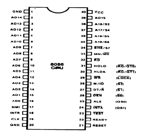
AD15-AD0: These are the time multiplexed memory I/O
address and data lines. Address remains on the lines during T1 state, while
the data is available on the data bus during T2, T3, Tw and T4. output address during the first part of bus cycle and input or output data during the remaining part of bus cycle.
A19/S6,A18/S5,A17/S4,A16/S3:
These are the time multiplexed address and status lines. During T1 these
are the most significant address lines for memory operations. During
the first part of the bus cycle the upper 4 bits of the address are output and
during the remainder of the bus cycle status is output. S3 and S4 indicates the
segment register being used as follows;

S6 : always remain a logic 0S5 : indicate condition of IF flag bits
RDRead: This signal on low indicates the peripheral that the processor is performing memory or I/O read operation.Data bus receive data from memory or
I/O device when RD=0
READY: This is the acknowledgement from the slow device or memory that they have completed the data transfer.
INTR-Interrupt Request: This is a triggered input. This is sampled during the last clock cycles of each instruction to determine the availability of the request. If any interrupt request is pending, the processor enters the interrupt acknowledge cycle.
TEST: Used in conjuction with the WAIT instruction in
multiprocessing environments. If the TEST pin goes low, execution will continue, else the processor remains in an idle state. The input is synchronized internally during each clock cycle on leading edge of clock.
CLK- Clock Input: Generates clock signals that synchronize the
operation of processor.The clock input provides the basic timing for processor operation and bus control activity.
Vcc: Supply voltage - +5 v ± 10%
GND: Ground
MN/MX: The logic level at this pin decides whether the processor is to operate in either minimum or maximum mode.Cpu is in minimum mode when strapped to +5 v and
in maximum mode when grounded.
BHE/S7: The bus high enable is used to indicate the transfer of data over the higher order ( D15-D8 ) data bus as shown in table. It goes low for the data transfer over D15-D8 and is used to derive chip selects of odd address memory bank or peripherals.If o during first of bus cycle this pin
indicates that at least one byte of the current transfer is to be made on pins
AD15-AD8 if 1 the transfer is made on AD7-AD0. Status s7 is output during the
latter part of bus assigned a meaning
Operation BHE AD0
Whole word 0 0
Upper byte from or to even address 0 1
Lower byte from or to even address 1 0
None 1 1
The following pin functions are for the minimum mode operation of 8086.
M/IO – Memory/IO: This is a status line logically equivalent to S2 in maximum mode. When it is low, it indicates the CPU is having an I/O operation, and when it is high, it indicates that the CPU is having a memory operation.
INTAInterrupt Acknowledge: This signal is used as a read strobe for interrupt acknowledge cycles. i.e. when it goes low, the processor has accepted the interrupt.
ALE – Address Latch Enable: This output signal indicates the availability of the valid address on the address/data lines, and is connected to latch enable input of latches.Mostly used to demultiplex the address and data lines.
DT/R – Data Transmit/Receive: This output is used to decide the direction of data flow through the transreceivers (bidirectional buffers). when DT/R=1 transreceiver transmit the data and when DT/R’=0 it receive the data.
DEN – Data Enable: This signal indicates the availability of valid data over the address/data lines. It is used to enable the transreceivers ( bidirectional buffers ) to separate the data from the multiplexed address/data signal.
HOLD, HLDA- Acknowledge: When the HOLD line goes high, it indicates to the processor that another master is requesting the bus access.The processor, after receiving the HOLD request, issues the hold acknowledge signal on HLDA pin, in the middle of the next clock cycle after completing the current bus cycle.
The following pin function are applicable for maximum mode operation of 8086.
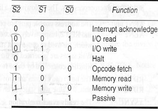
S2, S1, S0 – Status Lines: These are the status lines which reflect the type of operation, being carried out by the processor.
Bus control functions generated by Bus controller(8288) using status signal S2, S1, S0 shown in fig.
LOCK: This output pin indicates that other system bus master will be prevented from gaining the system bus, while the LOCK signal is low.
QS1, QS0 – Queue Status: These lines give information about the status of the code-prefetch queue.

RQ/0GT,RQ/1GT – Request/Grant: These pins are used by the other local bus master in maximum mode, to force the processor to release the local bus at the end of the processor current bus cycle.Each of the pin is bidirectional with RQ/GT0 having higher priority than RQ/GT1.
