Sunday 29 May 2016

Intel Core i5 vs. i7

For many consumers who want to buy a new PC or Laptop PC, one of the biggest question is related to the configuration i.e. type of Processor and memory. Top most Two CPUs often in considered for PC are the Intel Core i5 and Intel Core i7.
Intel’s Core i5 and i7 processors are faster in market, power efficient and better designed for modern computing than any others CPU. Now in world huge number of laptops and desktops consists of   i5s and i7s processor.
This post is written to help you decide whether you need to purchase the Core i7 or Core i5 based on different factor such as integrated graphics, clock speed, and hyper threading.

Price:
When we consider the price, there’s a clear difference between the two series, with some of the i5 chips are cheap as compare to i7 chips. Core i5-equipped systems will be less expensive than Core i7-equipped PCs.

Higher clocks: 
The clock speed is a common measure of how quickly each core on a processor can handle operations. so a higher clock speed means better performance. Intel’s dual-core i7 chips typically have higher clock speeds than their Core i5 counterparts, even at the same TDP. The fastest dual-core Core i7, which runs at 2.6GHz base and 3.2GHz standard. Where fastest Core i5 has a base clock of 2.3GHz and a max clock of 2.9GHz. The Core i7 processors have more capabilities than Core i5 CPUs.

Core:
For the most of operation, you'll get faster CPU performance from Core i7 than Core i5. The mostly of Core i7 desktop CPUs are quad-core processors, while many mobile Core i5 processors are dual core. This is not always the case, it may be dual-core mobile Core i7 processors and several quad-core desktop Core i5 CPUs.

More cache: 
Core i7 chips available with either 6MB or 4MB of cache. Core i5 chips available with 3MB or 4MB of cache. The i5 processors have in modern terms, when it comes to cache, this number smaller than most i7 processors by 2MB so it help the processor deal with repetitive tasks faster.

Hyper-Threading:
Hyper-Threading technology uses multithreading technology to increase performance on multithreaded tasks. The multithreading means a user running several programs simultaneously, but there are other activities that take advantage of Hyper-Threading, like multimedia operations.
In Hyper-Threading simplest situation is each core on the processor is capable of handling two threads instead of just one. Hyper-Threading technology is not found on Core i5 desktop chips. Where All Core i7 processors is build with Hyper-Threading technology, which means they all can handle twice as many threads as they have cores.

Wednesday 25 May 2016

Top 25 engineering colleges in India

The Human Resource Development (HRD) Ministry’s ‘India Ranking Report 2016’ has released the top engineering colleges in india. The ‘India Rankings 2016’ were ranked by National Bureau of Accreditation (NBA) based on five criteria — teaching and learning resources, graduation outcome, perception, outreach and inclusivity and research productivity. The ‘India Rankings 2016’ put together with the participation of 3,500 private and public institutions. All institutions were judged based on self-disclosure of information. The IITs have occupied the top 10 best engineering colleges slot with IIT Madras placed at number one. for more information visit at: http://indianexpress.com/article/education/top-25-engineering-colleges-in-india-nirf-ranking-2016/

Check out the top 25 engineering colleges in India

  1. Indian Institute of Technology Madras 
  2. Indian Institute of Technology Bombay 
  3. Indian Institute of Technology Delhi 
  4. Indian Institute of Technology Kharagpur 
  5. Indian Institute of Technology Kanpur 
  6. Indian Institute of Technology Roorkee 
  7. Indian Institute of Technology Hyderabad 
  8. Indian Institute of Technology Gandhinagar 
  9. Indian Institute of Technology Ropar 
  10. Indian Institute of Technology Patna 
  11. Indian Institute of Technology Guwahati 
  12. National Institute of Technology Tiruchirappalli 
  13. Vellore Institute of Technology, Vellore 
  14. Indian Institute of Technology (BHU), Varanasi 
  15. Sardar Vallabhbhai National Institute of Technology Surat 
  16. Indian Institute of Technology Indore 
  17. Birla Institute of Technology, Ranchi 
  18. Visvesvarya National Institute of Technology Nagpur 
  19. National Institute of Technology Rourkela 
  20. Indian Institute of Technology Mandi 
  21. College of Engineering, Pune 
  22. National Institute of Technology Karnataka Manglore 
  23. Motilal Nehru National Institute of Technology Allahabad 
  24. PSG College of Technology, Coimbatore 
  25. Indian Institute of Technology Jodhpur

Thursday 30 May 2013

The 8086 Pin Diagram

Signal Description of 8086

       The Microprocessor 8086 is a 16-bit CPU available in different clock rates and packaged a 40 pin CERDIP. The 8086 operates in single processor or multiprocessor configuration to achieve high performance.The pins serve a particular function in minimum mode (single processor mode) and other function in maximum mode configuration
AD15-AD0: These are the time multiplexed memory I/O address and data lines. Address remains on the lines during T1 state, while the data is available on the data bus during T2, T3, Tw and T4. output address during the first part of bus cycle and input or output data during the remaining part of bus cycle.
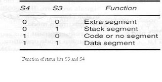
A19/S6,A18/S5,A17/S4,A16/S3: These are the time multiplexed address and status lines. During T1 these are the most significant address lines for memory operations. During the first part of the bus cycle the upper 4 bits of the address are output and during the remainder of the bus cycle status is output. S3 and S4 indicates the segment register being used as follows;

S6 : always remain a logic 0S5 : indicate condition of IF flag bits
RDRead: This signal on low indicates the peripheral that the processor is performing  memory or I/O read operation.Data bus receive data from memory or I/O device when RD=0
READY: This is the acknowledgement from the slow device or memory that they have completed the data transfer.
INTR-Interrupt Request: This is a triggered input. This is sampled during the last clock cycles of each instruction to determine the availability of the request. If any interrupt request is pending, the processor enters the interrupt acknowledge cycle.
TEST: Used in conjuction with the WAIT instruction in multiprocessing environments. If the TEST pin goes low, execution will continue, else the processor remains in an idle state. The input is synchronized internally during each clock cycle on leading edge of clock.
CLK- Clock Input: Generates clock signals that synchronize the operation of processor.The clock input provides the basic timing for processor operation and bus control activity.
Vcc: Supply voltage - +5 v ± 10%
GND: Ground
MN/MX: The logic level at this pin decides whether the processor is to operate in either minimum or maximum mode.Cpu is in minimum mode when strapped to +5 v and in maximum mode when grounded.
BHE/S7: The bus high enable is used to indicate the transfer of data over the higher order ( D15-D8 ) data bus as shown in table. It goes low for the data transfer over D15-D8 and is used to derive chip selects of odd address memory bank or peripherals.If o during first of bus cycle this pin indicates that at least one byte of the current transfer is to be made on pins AD15-AD8 if 1 the transfer is made on AD7-AD0. Status s7 is output during the latter part of bus assigned a meaning
Operation                                                 BHE       AD0                
Whole word                                                 0           0                      

Upper byte from or to even address              0           1                     

Lower byte from or to even address             1           0                     

None                                                           1          1                      
                                                           
The following pin functions are for the minimum mode operation of 8086.

M/IO – Memory/IO: This is a status line logically equivalent to S2 in maximum mode. When it is low, it indicates the CPU is having an I/O operation, and when it is high, it indicates that the CPU is having a memory operation.
INTAInterrupt Acknowledge: This signal is used as a read strobe for interrupt acknowledge cycles. i.e. when it goes low, the processor has accepted the interrupt.
ALE – Address Latch Enable: This output signal indicates the availability of the valid address on the address/data lines, and is connected to latch enable input of latches.Mostly used to demultiplex the address and data lines.
DT/R – Data Transmit/Receive: This output is used to decide the direction of data flow through the transreceivers (bidirectional buffers). when DT/R=1 transreceiver  transmit the data and when DT/R’=0 it receive the data.
DEN – Data Enable: This signal indicates the availability of valid data over the address/data lines. It is used to enable the transreceivers ( bidirectional buffers ) to separate the data from the multiplexed address/data signal.
HOLD, HLDA- Acknowledge: When the HOLD line goes high, it indicates to the processor that another master is requesting the bus access.The processor, after receiving the HOLD request, issues the hold acknowledge signal on HLDA pin, in the middle of the next clock cycle after completing the current bus cycle.
The following pin function are applicable for maximum mode operation of 8086.
S2, S1, S0 – Status Lines: These are the status lines which reflect the type of operation, being carried out by the processor.
Bus control functions generated by Bus controller(8288) using status signal S2, S1, S0 shown in fig.
LOCK: This output pin indicates that other system bus master will be prevented from gaining the system bus, while the LOCK signal is low.
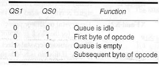
QS1, QS0 – Queue Status: These lines give information about the status of the code-prefetch queue.

RQ/0GT,RQ/1GT – Request/Grant: These pins are used by the other local bus master in maximum mode, to force the processor to release the local bus at the end of the processor current bus cycle.Each of the pin is bidirectional with RQ/GT0 having higher priority than RQ/GT1.


8086 Features & Architecture

Features of 8086 Microprocessor:
i)  It is a 16 bit processor, contains approximately 29,000 transistors & fabricated using HMOS technology.
ii)  The number of address lines are 20, so addressing capability of this is 220 = 1 MB.
iii)It has 20 address lines in which 16 lines are multiplexed with data lines.
iv) There are 16 control lines for providing the handshaking signals during bus transfer & for permitting at least some control to CPU.
v)  It requires only +5v DC supply.
vi)Its operating frequency is above 5 MHz (8086-1 requires operating frequency of 10 MHz & 8086-2 requires operating frequency of 8 MHz)
vii) In 40 pin configuration it has provided with two ground pins, pin no 1 & pin no 20.
viii) Input output current levels yield 350mV noise immunity for logic 0 (Output max can be as high as 450 mV while input max can be no higher than 800mV). This limits the loading on the outputs.

Architecture of 8086:


Above Figure  shows the internal architecture of 8086. It is divided in mainly two groups named as Execution Unit(EU) & Bus Interface Unit(BIU). 
The EU contains Data registers, 16 bit ALU, PSW, Control Logic. The BIU contains Segment registers, Instruction queue, Stack Pointer Registers & Index Register.
           The control unit working registers are divided into three groups according to their functions. There are data group, which is set of arithmetic registers, the pointer group, which include base & index registers,  stack pointer & the segment group which is a set of special base registers. 
          The data group consists of the AX, BX, CX, DX registers. These registers are used to store operands & result of operations. AX, BX, CX, DX registers are  used as 16 bit registers but they can be also used as 8 bit registers as:
            AX:- AL & AH
            BX:- BL & BH
            CX:- CL & CH
            DX:- DL & DH
      The pointer & index group consists of IP, SP, BP, SI & DI registers. The IP(Instruction Pointer) & SP(Stack Pointer) registers are essentially the program counter & stack pointer but the complete instruction& addresses are formed by adding the contents of these registers to the contains of code segments(CS) & stack segments(SS).BP is base register for accessing the stack SI & DI registers for indexing. The segment group consists of Code, Data, Extra, Stack Segments.

Flag register of 8086:
         A flag is a flip-flop which indicates some conditions produced by the execution of an instruction or controls certain operations of EU. A 16 bit flag register in EU contains nine active flags. These flags are as follows.
U
U
U
U
OF
DF
IF
TF
SF
ZF
U
AF
U
PF
U
CF
   15      14      13      12       11     10      09      08      07      06       05     04       03      02     01       00    

The flag register has two categories in itself
1)      Conditional flags including carry flag(CF), parity flag(PF), auxiliary carry flag(AF), sign flag(SF), zero flag(ZF), overflow flag(OF).
2)      Control flags including direction flag(DF), interrupt flag(IF), trap flag(TF)

The description for the above flag register according to the numbers below is specified here.
i) Sign flag:- It indicates whether the result of operation is positive or negative.
ii) Zero flag:- It is set when the result of arithmetic operation is zero.
iii) Parity flag:- It is set when the low order 8 bit of the result contains an even number of 1’s.
iv) Carry flag:- It is set when the carry/borrow is generated after arithmetic operations.
v)  Auxillary Carry flag:- Set, if there is carry/borrow by bit 3 during addition/subtraction.
vi) Overflow flag:- It is set if there is a carry generated from D7 bit to D8 bit.
vii) Direction flag:- It is set if the direction of data accessing starts from higher address otherwise starts from lower address.
viii) Interrupt flag:- If interrupt is generated during the execution this flag is set.
ix) Trap flag:- If set then the NMI interrupt will be present otherwise if the NMI pin is high this condition is false.